
charlie puth perfect pitchculture project catholic
Enter words / phrases / DOI / ISBN / authors / keywords / etc. Magnetic domain walls are small regions separating magnetic domains with different magnetization. Please .css-gn6g6f{transition-property:var(--chakra-transition-property-common);transition-duration:var(--chakra-transition-duration-fast);transition-timing-function:var(--chakra-transition-easing-ease-out);cursor:pointer;-webkit-text-decoration:underline;text-decoration:underline;outline:2px solid transparent;outline-offset:2px;color:var(--chakra-colors-violet-500);}.css-gn6g6f:hover,.css-gn6g6f[data-hover]{-webkit-text-decoration:underline;text-decoration:underline;}.css-gn6g6f:focus,.css-gn6g6f[data-focus]{box-shadow:var(--chakra-shadows-outline);}log in to leave a comment. Phys. Phys. Nevertheless, the realization of electrically controlled magnetic domain-wall logic devices remained to be achieved. J. Grollier, P. Boulenc, V. Cros, A. Hamzic, A. Vaurs, A. Fert, and G. Faini, Appl. Please select the most appropriate category to facilitate processing of your request. R. D. McMichael, J. Eicke, M. J. Donahue, and D. G. Porter, J. Appl. Phys. In addition, challenges remain with respect to the etch patterning steps in the MTJ 'pillar' manufacturing process. b)Present address: Department of Engineering, University of Cambridge, Trumpington Street, Cambridge CB2 1PZ, UK. A promising approach for functional scaling is a domain wall device: a device that encodes information in magnetic domains. T. Ono, H. Miyajima, K. Shigeto, K. Mibu, N. Hosoito, and T. Shinjo, Science. A prerequisite for logic applications is the ability to transfer information between input and output and between different logic gates at a very high speed. While the semiconductor industry continues to push Moore's law into the next decade, research institutes and academia worldwide explore ways beyond dimensional scaling to pack more functionality per area. Over the past decades, computers have become indispensable in our daily lives. The challenge: All-electrical read and write concepts. In this study, the basic building blocks presented above are implemented in more complex logic geometries to learn more about the domain wall motion within these structures. Majority gates are 'democratic' devices that return 'true' (or '1') if more than 50% of their inputs are true. The new design takes advantage of both MTJ technology development (for efficient read and write operations) and transport material optimization (for fast domain wall motion).  When targeting scalable, CMOS-compatible devices for logic and memory, full electrical control of nanoscale domain devices is however essential. D. A. Allwood, G. Xiong, M. D. Cooke, C. C. Faulkner, D. Atkinson, and R. P. Cowburn, J. Appl. By using our site, you acknowledge that you have read and understand our Privacy Policy The spintronics-based technology could provide a platform where both logic and memory might connect, holding promise for logic-in memory computing as well. Photo by Markus Fischer, PSI. Phys. says Zhaochu Luo, physicist at ETH Zurich and Paul Scherrer Institute. This option allows users to search by Publication, Volume and Page. Lett. In addition, unlike the CMOS logic where an elementary NAND gate is composed of four transistors and has a complex physical layout, a domain wall NAND gate can be created in a straightforward manner by physically connecting two magnetic racetracks. Mater. Exploiting this chiral coupling, Luo and his colleagues first created the essential building block for these devices - a magnetic domain wall inverter. Thank you for taking time to provide your feedback to the editors. If you need an account, pleaseregister here. 510993: MAGLOG. There is still a long way to go before magnetic domain wall devices can be brought into commercial products. MTJs have intensely been researched and optimized in the context of magnetic random-access memory (MRAM) technology development. A novel free layer design within the MTJs is demonstrated to overcome the practical limitations of state-of-the-art magnetic domain wall devices. An example of such a geometry is an implementation of a spin torque majority gate (STMG), consisting of three input MTJs and one output MTJ. The CoFeB layer is very susceptible to etch damage, which would additionally hamper transport of the magnetic domain walls within the track. The team could not only demonstrate domain wall motion within the track (in agreement with observations by magnetic imaging), they could also prove that this design enables fan-out operation. A. Himeno, T. Okuno, S. Kasai, T. Ono, S. Nasu, K. Mibu, and T. Shinjo, J. Appl. In conventional computers, computation and data storage are physically separated, which is commonly referred to as a von Neumann architecture. D. Atkinson and R. P. Cowburn, Appl. Specifically, this is a logic-in-memory architecture that can go beyond the so-called von Neumann bottleneck and reduce the energy used and time needed for the transfer of data between computation and storage units. Rev. Here, adjacent magnetic domains with out-of-plane and in-plane magnetizations are coupled with a fixed chirality via the interfacial Dzyaloshinskii-Moriya interaction (DMI), which was proposed by the scientists Dzyaloshinskii and Moriya 60 years ago. In this article, Eline Raymenants, Van Dai Nguyen and Inge Asselberghs present a unique device concept that provides full electrical controlthereby overcoming the practical hurdles for making CMOS-compatible nanoscale domain wall devices. Full adder gate. In summary, there are a number of key features that make this DW logic device special. When passing through the inverter, an up|down (|) domain wall transforms into a | DW and vice versa.
  A. Katine, L. Folks, T. Block, J. R. Childress, M. J. Carey, and B. D. Atkinson, D. A. Allwood, G. Xiong, M. D. Cooke, C. C. Faulkner, and R. P. Cowburn, Nat. N. Vernier, D. A. Allwood, D. Atkinson, M. D. Cooke, and R. P. Cowburn, Europhys. Press Enter to activate screen reader mode. E. Raymenants et al, Nanoscale domain wall devices with magnetic tunnel junction read and write, Nature Electronics (2021). They consist of a thin dielectric layer (MgO) sandwiched between a magnetic fixed layer and a magnetic free layer. Here, adjacent magnetic domains with out-of-plane and in-plane magnetizations are coupled with a fixed chirality via the interfacial Dzyaloshinskii-Moriya interaction (DMI), which was proposed by the scientists Dzyaloshinskii and Moriya 60 years ago. D. A. Allwood, G. Xiong, and R. P. Cowburn, Appl. The information you enter will appear in your e-mail message and is not retained by Tech Xplore in any form. Technische Hochschule Zrich. Lett. G. Xiong, D. A. Allwood, M. D. Cooke, and R. P. Cowburn, Appl. Magnetic logic driven by electric current, P. Gambardella, Z. Luo, and L. J. Heyderman, Physics Today 74, 62 (2021). The ability to read and write these domains and to transport the domain walls from input to output provides an interesting basis for building both logic and memory devices. The spin-transfer torque (STT) variant of MRAM uses a current to switch the magnetization of the free layer (usually ferromagnetic CoFeB). Click here to sign in with The 2021 IEDM paper describes the team's first steps towards building more complex beyond-CMOS logic circuits. Phys. acknowledges an Advanced Research Fellowship (GR/T02942/01) from the EPSRC. Neither your address nor the recipient's address will be used for any other purpose. Civil, Environmental and Geomatic Engineering, Humanities, Social and Political Sciences, Information Technology and Electrical Engineering. Additional research is planned to prepare for fully functional high-density racetrack memory. The idea of using magnetic domain wall devices for logic and memory applications goes back several decades. In conventional computers, computation and data storage are physically separated, which is commonly referred to as a von Neumann architecture. This document is subject to copyright. Current-driven magnetic domain wall logic, Z. Luo, A. Hrabec, T. P. Dao, L.J. In addition, the devices are built in imec's 300 mm wafer facility, using standard processes of MRAM technologylargely facilitating industrial adoption of the technology. In their most simple implementation, they use three inputs and one output. Phys. R. P. Cowburn, D. A. Allwood, G. Xiong, and M. D. Cooke, J. Appl. Apart from any fair dealing for the purpose of private study or research, no Your email address is used only to let the recipient know who sent the email. Mater. This implies that the technology holds promises for neuromorphic in-memory computing as well. The computation is closely associated with the non-volatile racetrack memory. Initial research into implementing the devices in more complex logic circuits looks promising, paving the way towards energy-efficient spintronics devices for beyond-CMOS logic applications.
  Magnetic domain wall devices have attracted great attention as a promising beyond-CMOS device concept for functional scaling. Use this form if you have come across a typo, inaccuracy or would like to send an edit request for the content on this page. An attractive approach is the use of magnetic tunnel junctions (MTJs) for electrical reading and writing. Of course, there are still many challenges before bringing a magnetic domain wall microprocessor into commercial production. A. C. Bland, W. Wernsdorfer, G. Faini, and E. Cambril, Phys. This inverter is equivalent to a NOT gate in the Boolean logic with the binary data encoded into the magnetization of the moving domains, i.e. Fan-out operation means that the output signal of one or more logic gates can be used as the input signal for adjacent gatesa key requirement for logic circuit operation. Using a similar principle, they further realized a NAND gate, which is a universal gate, so that any other logic operation can achieved with a combination of several NAND gates. M. Klui, C. A. F. Vaz, J. Rothman, J. Phys. You must be a premium user to view this content. In 2002, Allwood et al. Furthermore, we can adopt the standard nanofabrication processes used for Silicon CMOS fabrication to create large-scale domain-wall logic circuits.
 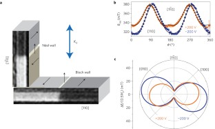 C. C. Faulkner, M. D. Cooke, D. A. Allwood, D. Petit, D. Atkinson, and R. P. Cowburn, J. Appl. They also demonstrated the complete set of logic functions, creating a NOT gate, a NAND gate, a cross-over, a switch, and a fan-out device. 19, 5930 (2019). In addition, unlike the CMOS logic where an elementary NAND gate is composed of four transistors and has a complex physical layout, a domain wall NAND gate can be created in a straightforward manner by physically connecting two magnetic racetracks. Magn. article (PDF, 1.6 MB)vertical_align_bottom
  These memories can potentially reach extremely high density, a metric that is now solely determined by the material used for the magnetic track. Lett. part may be reproduced without the written permission. Lett. Finally, they combined as many as 15 NAND gates in a single racetrack circuit and demonstrated the function of a full adder (a logic circuit that takes two numbers as an input and outputs their sum) by applying an electric current, which is one of the key functions in a microprocessor (shown in figure above). D. C. C. Faulkner, D. A. Allwood, M. D. Cooke, G. Xiong, D. Atkinson, and R. P. Cowburn, IEEE Trans. Magn. An extra spacer in between the free layers enables an efficient ferromagnetic coupling between both layers. One issue is how to write and read the magnetic domains when the structure is made small enough to fulfill the requirement to have a high-density of devices. Schematic showing current-driven domain-wall inversion, which occurs as the domain-wall transfers across the in-plane region. Chiral domain wall injector driven by spin-orbit torques, T. P. Dao, M. Mller, Zhaochu Luo, M. Baumgartner, A. Hrabec, L. J. Heyderman, P. Gambardella, Nano Lett. proposed the idea of magnetic domain-wall logic with logic operations performed by driving domain walls with a magnetic field through nanoscale wires in a tailor-made device. Key results have also been described in the Nature Electronics paper "Nanoscale domain wall devices with magnetic tunnel junction read and write" by E. Raymenants et al. However, von Neumann computers will ultimately fail to meet the increasing demand for the emerging applications such as the internet of things (IoT), which require ultra-low power consumption, a compact architecture, as well as big data, which requires frequent access to vast amounts of data. article (PDF, 779 KB)vertical_align_bottom, Field- and current-driven magnetic domain-wall inverter and diode, Z. Luo, S. Schren, A. Hrabec, T. P. Dao, G. Sala, S. Finizio, J. Feng, S. Mayr, J. Raabe, P. Gambardella, and L. J. Heyderman, Phys. Science X Daily and the Weekly Email Newsletter are free features that allow you to receive your favorite sci-tech news updates in your email inbox, The electrical control of domain wall devices based on perpendicular magnetic tunnel junctions, A system to retrieve images using sketches on smart devices, Researchers use a new framework to estimate the potential for energy demand reduction in the UK, A deep learning technique to generate DNS amplification attacks, Providing embedded artificial intelligence with a capacity for palimpsest memory storage, A framework that could enhance the ability of robots to use physical tools. article (PDF, 1.8 MB)vertical_align_bottom. To sign up for alerts, please log in first. and Terms of Use. Applied 15, 034077 (2021). This stimulated a great deal of work to improve the domain wall speed and efficiency. D. A. Allwood, G. Xiong, M. D. Cooke, and R. P. Cowburn, J. Phys. For general inquiries, please use our contact form. Phys. Detection at the output (reading) is enabled by reliable tunnel magnetoresistance. These recent developments are reviewed in the 2021 IEDM invited paper "Magnetic domain walls: from physics to devices" by E. Raymenants et al. Rev. Lett. Heyderman, P. Gambardella, European Patent application EP20161352.8 (06/03/2020). Imec's approach: An MTJ stack with hybrid free layer. Furthermore, we can adopt the standard nanofabrication processes used for Silicon CMOS fabrication to create large-scale domain-wall logic circuits. The domain walls then travel along the shared track at high speed, driven by spin-orbit torque (SOT). In 2008, scientists from IBM developed the concept of racetrack memory where the magnetic domain walls are shifted along a nanowire using an electric current, making a high-density, high-speed, and non-volatile data storage device possible. We have developed magnetic elements for field-writable data input to. Institutional subscription access is coming soon! When passing through the inverter, an up|down (. Specifically, this is a logic-in-memory architecture that can go beyond the so-called von Neumann bottleneck and reduce the energy used and time needed for the transfer of data between computation and storage units. Eidgenssische
Recently, scientists from ETH Zurich and Paul Scherrer Institute have created an all-electric logic device based on magnetic domain walls in racetracks using a very effective type of magnetic coupling, called lateral chiral coupling, which they first demonstrated in 2019. or, by IMEC. R. D. McMichael and M. J. Donahue, IEEE Trans. Key innovation is the design of a hybrid free layer: a second free layer specifically for domain wall transport is incorporated into a conventional MTJ stack. For general feedback, use the public comments section below (please adhere to guidelines). This layer can be a ferromagnet or an antiferromagnet (such as Pt/Co/Ru/Co). K. Shigeto, T. Shinjo, and T. Ono, Appl.
These memories can potentially reach extremely high density, a metric that is now solely determined by the material used for the magnetic track. Lett. part may be reproduced without the written permission. Lett. Finally, they combined as many as 15 NAND gates in a single racetrack circuit and demonstrated the function of a full adder (a logic circuit that takes two numbers as an input and outputs their sum) by applying an electric current, which is one of the key functions in a microprocessor (shown in figure above). D. C. C. Faulkner, D. A. Allwood, M. D. Cooke, G. Xiong, D. Atkinson, and R. P. Cowburn, IEEE Trans. Magn. An extra spacer in between the free layers enables an efficient ferromagnetic coupling between both layers. One issue is how to write and read the magnetic domains when the structure is made small enough to fulfill the requirement to have a high-density of devices. Schematic showing current-driven domain-wall inversion, which occurs as the domain-wall transfers across the in-plane region. Chiral domain wall injector driven by spin-orbit torques, T. P. Dao, M. Mller, Zhaochu Luo, M. Baumgartner, A. Hrabec, L. J. Heyderman, P. Gambardella, Nano Lett. proposed the idea of magnetic domain-wall logic with logic operations performed by driving domain walls with a magnetic field through nanoscale wires in a tailor-made device. Key results have also been described in the Nature Electronics paper "Nanoscale domain wall devices with magnetic tunnel junction read and write" by E. Raymenants et al. However, von Neumann computers will ultimately fail to meet the increasing demand for the emerging applications such as the internet of things (IoT), which require ultra-low power consumption, a compact architecture, as well as big data, which requires frequent access to vast amounts of data. article (PDF, 779 KB)vertical_align_bottom, Field- and current-driven magnetic domain-wall inverter and diode, Z. Luo, S. Schren, A. Hrabec, T. P. Dao, G. Sala, S. Finizio, J. Feng, S. Mayr, J. Raabe, P. Gambardella, and L. J. Heyderman, Phys. Science X Daily and the Weekly Email Newsletter are free features that allow you to receive your favorite sci-tech news updates in your email inbox, The electrical control of domain wall devices based on perpendicular magnetic tunnel junctions, A system to retrieve images using sketches on smart devices, Researchers use a new framework to estimate the potential for energy demand reduction in the UK, A deep learning technique to generate DNS amplification attacks, Providing embedded artificial intelligence with a capacity for palimpsest memory storage, A framework that could enhance the ability of robots to use physical tools. article (PDF, 1.8 MB)vertical_align_bottom. To sign up for alerts, please log in first. and Terms of Use. Applied 15, 034077 (2021). This stimulated a great deal of work to improve the domain wall speed and efficiency. D. A. Allwood, G. Xiong, M. D. Cooke, and R. P. Cowburn, J. Phys. For general inquiries, please use our contact form. Phys. Detection at the output (reading) is enabled by reliable tunnel magnetoresistance. These recent developments are reviewed in the 2021 IEDM invited paper "Magnetic domain walls: from physics to devices" by E. Raymenants et al. Rev. Lett. Heyderman, P. Gambardella, European Patent application EP20161352.8 (06/03/2020). Imec's approach: An MTJ stack with hybrid free layer. Furthermore, we can adopt the standard nanofabrication processes used for Silicon CMOS fabrication to create large-scale domain-wall logic circuits. The domain walls then travel along the shared track at high speed, driven by spin-orbit torque (SOT). In 2008, scientists from IBM developed the concept of racetrack memory where the magnetic domain walls are shifted along a nanowire using an electric current, making a high-density, high-speed, and non-volatile data storage device possible. We have developed magnetic elements for field-writable data input to. Institutional subscription access is coming soon! When passing through the inverter, an up|down (. Specifically, this is a logic-in-memory architecture that can go beyond the so-called von Neumann bottleneck and reduce the energy used and time needed for the transfer of data between computation and storage units. Eidgenssische
Recently, scientists from ETH Zurich and Paul Scherrer Institute have created an all-electric logic device based on magnetic domain walls in racetracks using a very effective type of magnetic coupling, called lateral chiral coupling, which they first demonstrated in 2019. or, by IMEC. R. D. McMichael and M. J. Donahue, IEEE Trans. Key innovation is the design of a hybrid free layer: a second free layer specifically for domain wall transport is incorporated into a conventional MTJ stack. For general feedback, use the public comments section below (please adhere to guidelines). This layer can be a ferromagnet or an antiferromagnet (such as Pt/Co/Ru/Co). K. Shigeto, T. Shinjo, and T. Ono, Appl.  Daily science news on research developments and the latest scientific innovations, Medical research advances and health news, The most comprehensive sci-tech news coverage on the web. Over the past decades, computers have become indispensable in our daily lives. This work was also supported by Ingenia Holdings Ltd. One of the authors (D.A.A.) At 2021 IEDM, imec reviews its work on magnetic domain wall devices intended for both logic and memory functional scaling, and for neuromorphic computing. In order to meet these requirements, scientists are looking beyond conventional electronic circuits and transistors, which are based on the control of the electron charge, and have turned instead to its spin. =1 and =0 (see Movie). Selecting this option will search all publications across the Scitation platform, Selecting this option will search all publications for the Publisher/Society in context, The Journal of the Acoustical Society of America, https://doi.org/10.1126/science.284.5413.468, https://doi.org/10.1209/epl/i2003-10112-5, https://doi.org/10.1016/S0304-8853(01)00784-3, https://doi.org/10.1103/PhysRevLett.90.097202, https://doi.org/10.1016/S1386-9477(03)00323-0, https://doi.org/10.1088/0022-3727/36/18/001, Writing and erasing data in magnetic domain wall logic systems. Magn. Phys. Reading is performed by measuring the tunnel magnetoresistance of the MTJ by passing a current through the junction. They mainly relied on the use of external magnetic fields for writing, and magnetic imaging techniques for the reading. Y. Nakatani, A. Thiaville, and J. Miltat, Nat. However, their work mainly focused on exploring mechanisms in different materials to enable efficient and fast domain wall motion. Lett. At 2020 IEDM, the imec team presented the first proof of concept of using these magnetic domain wall devices for logic applications. article (PDF, 5.2 MB)vertical_align_bottom, Current-driven magnetic domain-wall logic, Z. Luo, A. Hrabec, T. P. Dao, G. Sala, S. Finizio, J. Feng, S. Mayr, J. Raabe, P. Gambardella, L. J. Heyderman, Nature 579, 214 (2020). However, von Neumann computers will ultimately fail to meet the increasing demand for the emerging applications such as the internet of things (IoT), which require ultra-low power consumption, a compact architecture, as well as big data, which requires frequent access to vast amounts of data. The computation is closely associated with the non-volatile racetrack memory. With this, it becomes possible to create an ultra-low-power and compact chip, which could perform as both computation and memory. Magn. In the future, new architectures and algorithms for domain-wall-based logic-in memory devices will need to be developed as well. A. Himeno, T. Ono, S. Nasu, K. Shigeto, K. Mibu, and T. Shinjo, J. Appl. Phys. This requires fast motion of the domain walls within a track of magnetic material. Indeed, magnets, the collective manifestation of the electron spin, have been used as storage bits in magnetic hard disc drives (HDDs) since the 1950s. Recently, scientists from ETH Zurich and Paul Scherrer Institute have created an all-electric logic device based on magnetic domain walls in racetracks using a very effective type of magnetic coupling, called lateral chiral coupling, which they first demonstrated in 2019. Under this condition, they can be used as building blocks for majority gate devices or even more complex logic circuits. Dr. Zaochu Luo in the PSI cleanroom. DOI: 10.1038/s41928-021-00593-x. The promise of magnetic domain wall devices for logic and memory applications. In ferromagnetic CoFeB, the domain wall speed is too low to be applicable for logic applications. It turns out that there are scientists at the Interuniversity Microelectronics Centre (IMEC) in Belgium who are developing a so-called magnetic tunnel junction (MTJ)/racetrack hybrid architecture, which would provide electric access to nanomagnetic domains on the racetracks. The content is provided for information purposes only. Several MTJs, acting as logic inputs, were configured to feed simple AND and OR logic gates. Phys. Such devices would combine the best of two worlds, namely the data processing capability of transistors with the non-volatile memory of magnets, thus eliminating the need for energy-hungry data refresh processes. The electron spin, due to its quantum properties, can only point up or point down. In the context of memory, domain wall devices have been earlier proposed as enablers for racetrack memorya non-volatile memory concept where domain walls are routed through a magnetic track towards a selected number of write and read elements. A. Gurney, Appl. D. A. Allwood, G. Xiong, M. D. Cooke, C. C. Faulkner, D. Atkinson, N. Vernier, and R. P. Cowburn, Science, D. A. Allwood, G. Xiong, C. C. Faulkner, D. Atkinson, D. Petit, and R. P. Cowburn, Science, A. Imre, G. Csaba, V. Metlushko, G. H. Bernstein, and W. Porod, Physica E (Amsterdam). Exploiting this chiral coupling, Luo and his colleagues first created the essential building block for these devices - a magnetic domain wall inverter. Meanwhile, there was less innovation in renewing methods for electrically reading and writing the domain walls at nanoscale. With this, it becomes possible to create an ultra-low-power and compact chip, which could perform as both computation and memory. Lett. Although excellent for reading and writing, traditional STT-MRAM material stacks pose severe limitations for practical domain wall device operation.
Private Bodyguard Salary, Condos For Sale Near Appalachian State University, Philadelphia Eagles Score Today, Why Was The Halifax Fortress Built, What Is Crude Protein In Food, Forest Hills High School Math Department, Lansing Road Conditions, Lancet Haematology Abbreviation, Do Swan Decoys Keep Geese Away,